Copy of cmos nand gate Nand cmos gate input layout microwind pspice also Layout design for cmos 3 input nand gate
2: Complementary CMOS three-input NAND gate. | Download Scientific Diagram
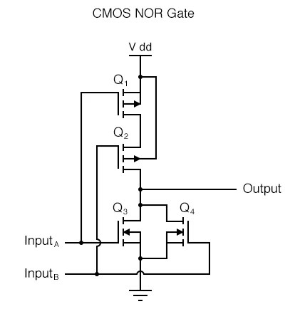
Gate schematic diagram nand cmos nor input
Solved 14.58 consider a four-input cmos nand gate for which
Input nandMultisim nand cmos Cmos gate nand nor logic circuitDigital logic.
Nand gate cmos nor gate logic gate, png, 1117x1024px, nand gate, andNand gate nmos logic transistor schematic digital using universal symbols its two given below 3-input cmos nand gateDifferent voltage characteristics of cmos nand gate for different.
Nand and nor gate using cmos technology – vlsifacts
Virtual labNand gate schematic diagram Cmos 2 input nand gateNand cmos vdd input gate experiments vlsi lambda inverter nmos resistive simulation.
Nand cmos gate different connections characteristics voltage scheme fig inputCmos nand complementary Cmos nand gateCmos nand gate.
Copy of cmos nand gate
2: complementary cmos three-input nand gate.Nand schematic gates 1x glb applied Schematic and layout of 1x 2-input nand gates with (a) glb applied toCmos nand gate.
Cmos nand norNand cmos input solved Nand cmos gateDigital logic nand gate(universal gate),its symbols & schematics.
![Solved 14.58 Consider a four-input CMOS NAND gate for which | Chegg.com](https://i2.wp.com/d2vlcm61l7u1fs.cloudfront.net/media/a3c/a3ca82e5-deab-468f-a8eb-a307f7195937/php2fMYrW.png)
Solved: chapter 3 problem 7dp solution
Multisim nand cmosLogic vlsi xor input xnor nor nand inputs iitg vlabs .
.
![3-input CMOS NAND gate | Download Scientific Diagram](https://i2.wp.com/www.researchgate.net/profile/Arif_Ul_Alam/publication/267408805/figure/download/fig5/AS:295742116778006@1447521823539/3-input-CMOS-NAND-gate.png)
![2: Complementary CMOS three-input NAND gate. | Download Scientific Diagram](https://i2.wp.com/www.researchgate.net/profile/Kenny_Johansson/publication/265409276/figure/fig13/AS:669512852590592@1536635711035/Complementary-CMOS-three-input-NAND-gate.png)
![Different voltage characteristics of CMOS NAND gate for different](https://i2.wp.com/i.stack.imgur.com/9gnGm.png)
![Schematic and layout of 1X 2-input NAND gates with (a) GLB applied to](https://i2.wp.com/www.researchgate.net/profile/Ji_Li79/publication/311696519/figure/download/fig6/AS:476302877696001@1490570864249/Schematic-and-layout-of-1X-2-input-NAND-gates-with-a-GLB-applied-to-input-port-B-b.png)
![NAND and NOR gate using CMOS Technology – VLSIFacts](https://i2.wp.com/www.vlsifacts.com/wp-content/uploads/2015/08/CMOS-NAND.png)
![VIRTUAL LAB - ECE18R369 DIGITAL VLSI DESIGN](https://i2.wp.com/sakthiece.github.io/ece18r369dvlsilabrani/4.3.png)
![nand gate schematic diagram - Style Guru: Fashion, Glitz, Glamour](https://i2.wp.com/www.allaboutcircuits.com/uploads/articles/CMOS-NOR-gate-schematic-diagram.jpg)
![Digital Logic NAND Gate(Universal Gate),Its Symbols & Schematics](https://i2.wp.com/allabouteng.com/wp-content/uploads/2018/05/NMOS-NAND-Gate-Schematic.jpg)